- 您现在的位置:买卖IC网 > Sheet目录2000 > IDTCV119EPVG8 (IDT, Integrated Device Technology Inc)IC CLK GEN DESKTOP PC 48-SSOP
COMMERCIALTEMPERATURERANGE
4
IDTCV119E
CLOCKGENERATORFORDESKTOPPCPLATFORMS
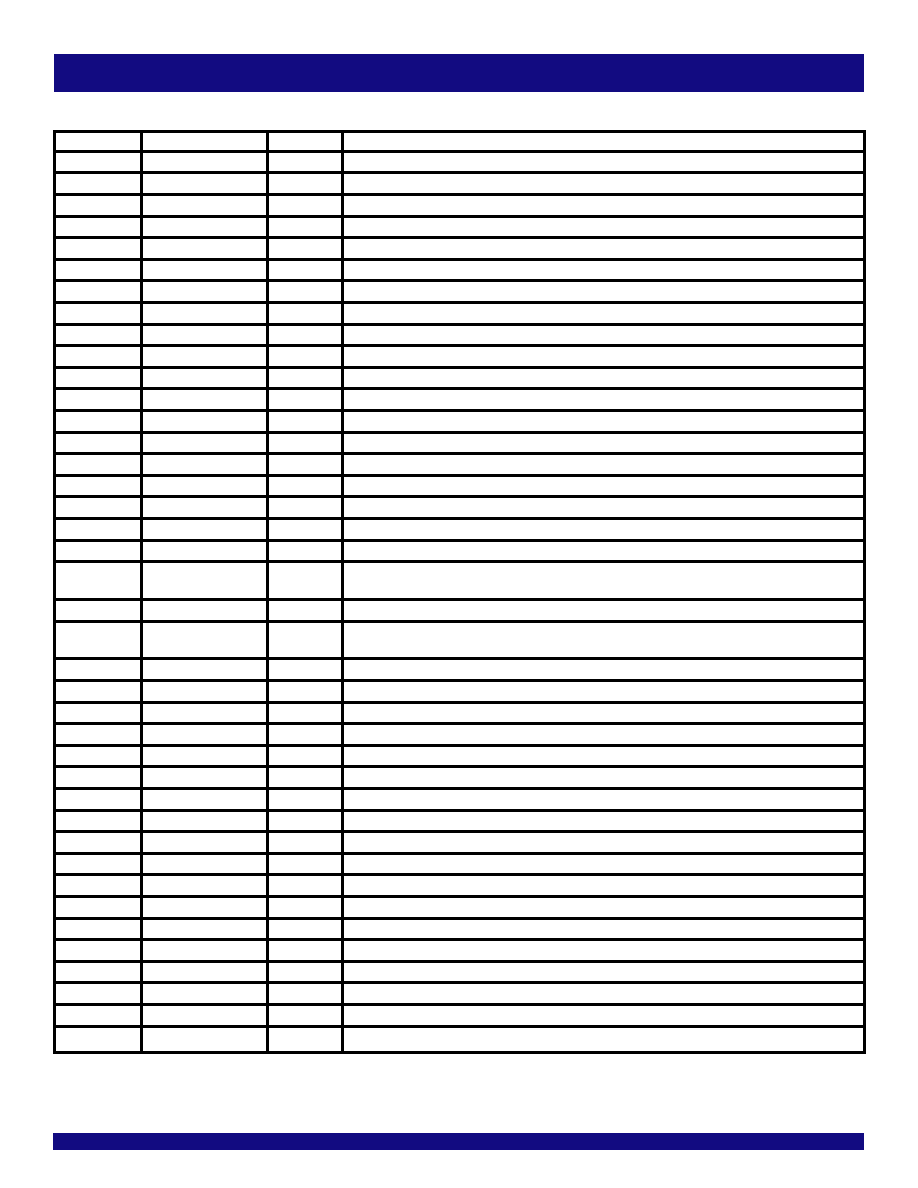
PIN DESCRIPTION
Pin Number
Name
Type
Description
1
FS1/REF0
I/O
Frequency select latch input 3.3V input HIGH/LOW voltage/ 14.318MHz reference clock output(1)
2
FS0/REF1
I/O
Frequency select latch input 2.5V input HIGH/LOW voltage/ 14.318MHz reference clock output(1)
3VDD_REF
PWR
3.3V
4
X1
I N
Xtalinput
5
X2
OUT
Xtaloutput
6VSS
GND
7
PCIF0
I/O
Frequency select latch input 3.3V input HIGH/LOW voltage/ PCI free running clock(2)
8
PCIF1
OUT
PCI free running clock
9
PCIF2
OUT
PCI free running clock
10
VDD_PCI
PWR
3.3V
11
VSS
GND
12
PCI0
OUT
PCI clock
13
PCI1
OUT
PCI clock
14
PCI2
OUT
PCI clock
15
PCI3
OUT
PCI clock
16
VDD_PCI
PWR
3.3V
17
VSS
GND
18
PCI4
OUT
PCI clock
19
PCI5
OUT
PCI clock
20
RESET#/PD#
OUT
Resetoutputsignalfromwatchdogcircuit,activeLOW/powerdowncontrolinput. Modeselectablethrough
SM bus, power on is RESET# mode.(1) Byte 34 bit 5.
21
SEL24/24_48MHz#
OUT
24/48MHz clock output, LOW 48MHz(2)
22
48MHz0
OUT
48MHz clock output. Phase is 180 different with 24_48, 48MHz1, and VCH. Output drive stength can
be doubled through SM programming.
23
VSS
GND
24
VDD48
PWR
3.3V
25
3V66_3/VCH
OUT
66MHz or 48MHz clock output. Selectable by SM Bus. Power on is 66MHz.
26
3V66_2
OUT
66MHz clock output
27
VDD_3V66
PWR
3.3V
28
VSS
GND
29
3V66_1
OUT
66MHz clock output
30
RESET#
OUT
RESET#
31
SCLK
I N
SMBus clock(1)
32
SDATA
I/O
SMBus data(1)
33
VTT_PWRGD#
I N
Used for power on latch, active LOW(1)
34
VDD_SRC
PWR
3.3V
35
SRCC
OUT
SATA 0.7V current mode differential clock output
36
SRCT
OUT
SATA 0.7V current mode differential clock output
37
VSS
GND
38
CPUC0
OUT
Hosts 0.7V current mode differential clock output
39
CPUT0
OUT
Hosts 0.7V current mode differential clock output
40
VDD_CPU
PWR
3.3V
NOTES:
1. ~ 130K
Ω internal pull-up.
2. ~ 130K
Ω internal pull-down.
发布紧急采购,3分钟左右您将得到回复。
相关PDF资料
IDTCV133PAG
IC FLEXPC CLK PROGR P4 56-TSSOP
IDTCV136PAG
IC FLEXPC CLK ATI RS400 56-TSSOP
IDTCV137PAG
IC FLEXPC CLK AMD K8 56-TSSOP
IDTCV142PAG
IC FLEXPC CLK PROGR P4 56-TSSOP
IDTCV146PVG
IC FLEXPC CLK PROGR P4 56-SSOP
IDTCV149PAG
IC FLEXPC CLK PROGR K8 56-TSSOP
IDTNW6005ASG
IC CALLER ID DECODER 20SOIC
IDTNW6006AS
IC CALLER ID DECODER 20-SOIC
相关代理商/技术参数
IDTCV122C
制造商:IDT 制造商全称:Integrated Device Technology 功能描述:PROGRAMMABLE FLEXPC? CLOCK FOR P4 PROCESSOR
IDTCV122CPVG
功能描述:IC FLEXPC CLK PROGR P4 56-SSOP RoHS:是 类别:集成电路 (IC) >> 时钟/计时 - 专用 系列:FlexPC™ 标准包装:28 系列:- 类型:时钟/频率发生器 PLL:是 主要目的:Intel CPU 服务器 输入:时钟 输出:LVCMOS 电路数:1 比率 - 输入:输出:3:22 差分 - 输入:输出:无/是 频率 - 最大:400MHz 电源电压:3.135 V ~ 3.465 V 工作温度:0°C ~ 85°C 安装类型:表面贴装 封装/外壳:64-TFSOP (0.240",6.10mm 宽) 供应商设备封装:64-TSSOP 包装:管件
IDTCV122CPVG8
功能描述:IC FLEXPC CLK PROGR P4 56-SSOP RoHS:是 类别:集成电路 (IC) >> 时钟/计时 - 专用 系列:FlexPC™ 标准包装:28 系列:- 类型:时钟/频率发生器 PLL:是 主要目的:Intel CPU 服务器 输入:时钟 输出:LVCMOS 电路数:1 比率 - 输入:输出:3:22 差分 - 输入:输出:无/是 频率 - 最大:400MHz 电源电压:3.135 V ~ 3.465 V 工作温度:0°C ~ 85°C 安装类型:表面贴装 封装/外壳:64-TFSOP (0.240",6.10mm 宽) 供应商设备封装:64-TSSOP 包装:管件
IDTCV123
制造商:IDT 制造商全称:Integrated Device Technology 功能描述:PROGRAMMABLE FLEXPC CLOCK FOR P4 PROCESSOR
IDTCV123PV
功能描述:IC FLEXPC CLK PROGR P4 56-SSOP RoHS:否 类别:集成电路 (IC) >> 时钟/计时 - 专用 系列:FlexPC™ 标准包装:1,500 系列:- 类型:时钟缓冲器/驱动器 PLL:是 主要目的:- 输入:- 输出:- 电路数:- 比率 - 输入:输出:- 差分 - 输入:输出:- 频率 - 最大:- 电源电压:3.3V 工作温度:0°C ~ 70°C 安装类型:表面贴装 封装/外壳:28-SSOP(0.209",5.30mm 宽) 供应商设备封装:28-SSOP 包装:带卷 (TR) 其它名称:93786AFT
IDTCV123PV8
功能描述:IC FLEXPC CLK PROGR P4 56-SSOP RoHS:否 类别:集成电路 (IC) >> 时钟/计时 - 专用 系列:FlexPC™ 标准包装:1,500 系列:- 类型:时钟缓冲器/驱动器 PLL:是 主要目的:- 输入:- 输出:- 电路数:- 比率 - 输入:输出:- 差分 - 输入:输出:- 频率 - 最大:- 电源电压:3.3V 工作温度:0°C ~ 70°C 安装类型:表面贴装 封装/外壳:28-SSOP(0.209",5.30mm 宽) 供应商设备封装:28-SSOP 包装:带卷 (TR) 其它名称:93786AFT
IDTCV123PVG
功能描述:IC FLEXPC CLK PROGR P4 56-SSOP RoHS:是 类别:集成电路 (IC) >> 时钟/计时 - 专用 系列:FlexPC™ 标准包装:1,500 系列:- 类型:时钟缓冲器/驱动器 PLL:是 主要目的:- 输入:- 输出:- 电路数:- 比率 - 输入:输出:- 差分 - 输入:输出:- 频率 - 最大:- 电源电压:3.3V 工作温度:0°C ~ 70°C 安装类型:表面贴装 封装/外壳:28-SSOP(0.209",5.30mm 宽) 供应商设备封装:28-SSOP 包装:带卷 (TR) 其它名称:93786AFT
IDTCV123PVG8
功能描述:IC FLEXPC CLK PROGR P4 56-SSOP RoHS:是 类别:集成电路 (IC) >> 时钟/计时 - 专用 系列:FlexPC™ 标准包装:28 系列:- 类型:时钟/频率发生器 PLL:是 主要目的:Intel CPU 服务器 输入:时钟 输出:LVCMOS 电路数:1 比率 - 输入:输出:3:22 差分 - 输入:输出:无/是 频率 - 最大:400MHz 电源电压:3.135 V ~ 3.465 V 工作温度:0°C ~ 85°C 安装类型:表面贴装 封装/外壳:64-TFSOP (0.240",6.10mm 宽) 供应商设备封装:64-TSSOP 包装:管件